

RAKESH ASERY
TYPICAL DESIGN FLOW
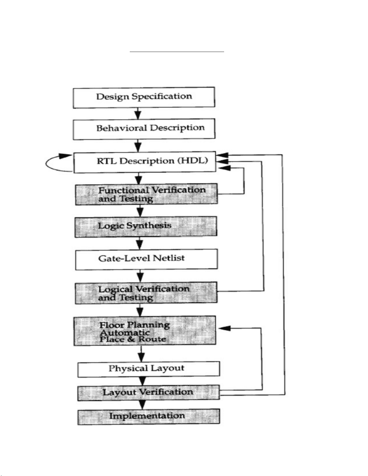
A typical design flow for designing VLSI IC circuits is shown in figure. Unshaded blocks show
the level of design representation, shaded blocks show process of design flow.

Study with the several resources on Docsity

Earn points by helping other students or get them with a premium plan

Prepare for your exams
Study with the several resources on Docsity
Earn points to download
Earn points by helping other students or get them with a premium plan
Community
Ask the community for help and clear up your study doubts
Discover the best universities in your country according to Docsity users
Free resources
Download our free guides on studying techniques, anxiety management strategies, and thesis advice from Docsity tutors
To Design Half Adder using Verilog and simulate, To Design Multiplexer 4x1 using Verilog and simulate, To Design Full Adder using Verilog and simulate, To Design D Flip-flop using Verilog and simulate, To Design JK Flip-flop using Verilog and simulate, To Design Counter using Verilog and simulate, To design two bit comparator in Verilog and simulate, To design 4-Bit Multiplier in Verilog and simulate,
Typology: Lab Reports
1 / 36

This page cannot be seen from the preview
Don't miss anything!
A typical design flow for designing VLSI IC circuits is shown in figure. Unshaded blocks show the level of design representation, shaded blocks show process of design flow.
Simulator.
The half-adder adds two inputs bits and generates a carry and sum, which are the two outputs of half-adder. The input variables of a half adder are called the augend and addend bits. The output variables are the sum and carry. The truth table for the half adder is:- S=AxorB C=AandB VERILOG CODE GATE LEVEL:- module RAKSHKAD(); reg A,B; wire C,S; ha_h(A,B,C,S); initial begin A=1'b0; B=1'b1;
Xilinx ISE Simulator
module RAKESHMUX4X1(i0, i1, i2, i3, s0, s1, out); input i0,i1,i2,i3,s0,s1; output out; wire y0,y1,y2,y3; wire s1n,s0n; not(s1n,s1); not(s0n,s0); and(y0,i0,s1n,s0n); and(y1,i1,s1n,s0); and(y2,i2,s1,s0n); and(y3,i3,s1,s0); or(out,y0,y1,y2,y3); endmodule DATA FLOW:- module RAKSHKMUX(out,i0,i1,i2,i3,s0,s1); output out; input i0,i1,i2,i3,s0,s1; assign out=(~s1&~s0&i0); assign out=(~s1&s0&i1); assign out=(s1&~s0&i2); assign out=(s1&s0&i3); endmodule
module RAKSHKMUXR4x1(out, i0, i2, i3, i1, s0, s1); output out; input i0,i1,i2,i3,s0,s1; reg out; always@(i0 or i1 or i2 or i3 or s0 or s1) case({s1,s0}) 2'b00: out=i0; 2'b01: out=i1; 2'b10: out=i2; 2'b11: out=i3; endcase endmodule SCHEMATIC DIAGRAM: -
Xilinx ISE Simulator.
Simulator.
The full-adder adds three inputs bits and generates a carry and sum, which are the two outputs of full adder. The input variables of a full adder are called the augend and addend bits. The output variables are the sum and carry. The truth table for the full adder is:- S=AxorBxorC CA=(AandB)or(BandC)or(CandA) VERILOG CODE GATE LEVEL:- module RAFULLADDER(a,b,c,sum,carry); output sum,carry; input a,b,c; wire w,x,y,z; xor(w,a,b); xor(sum,w,c); and(x,a,b);
3'b001:begin sum=1;carry=0;end 3'b010:begin sum=1;carry=0;end 3'b011:begin sum=0;carry=1;end 3'b100:begin sum=1;carry=0;end 3'b101:begin sum=0;carry=1;end 3'b110:begin sum=0;carry=1;end 3'b111:begin sum=1;carry=1;end endcase endmodule SCHEMATIC DIAGRAM: -
using Xilinx ISE Simulator.
begin if(D) Q<=1; else Q<=0; end endmodule SCHEMATIC DIAGRAM: -
using Xilinx ISE Simulator.
case({J,K}) 2'b 00:begin Q=Q; Qnot=Qnot; end 2'b 01:begin Q=0; Qnot=1; end 2'b 10:begin Q=1; Qnot=0; end 2'b 11:begin Q=~; Qnot=~Qnot; end endcase endmodule SCHEMATIC DIAGRAM: -
same using Xilinx ISE Simulator.