Download Propagation Delay -Components and Design Techniques for Digital System - Exams and more Exams Digital Systems Design in PDF only on Docsity!
University of California at Berkeley College of Engineering Department of Electrical Engineering and Computer Sciences
EECS150 J. Wawrzynek Spring 2003 4/4/
Exam II
Name: ________________________________________________________________
ID Number: ____________________________________________________________
This is a closed-book, closed note exam. No calculators please. You have 3 hours. Each
question is marked with its number of points (one point per expected minute of time).
Put your name and SID on each page. You can work out your answers on the backs of
the pages and use the extra blank sheets at the end of the booklet.
Show your work. Write neatly and be well organized.
Good luck!
problem maximum score
1 10pts
2 5pts
3 7pts
4 20pts
5 8pts
6 20pts
7 10pts
8 10pts
total 90pts
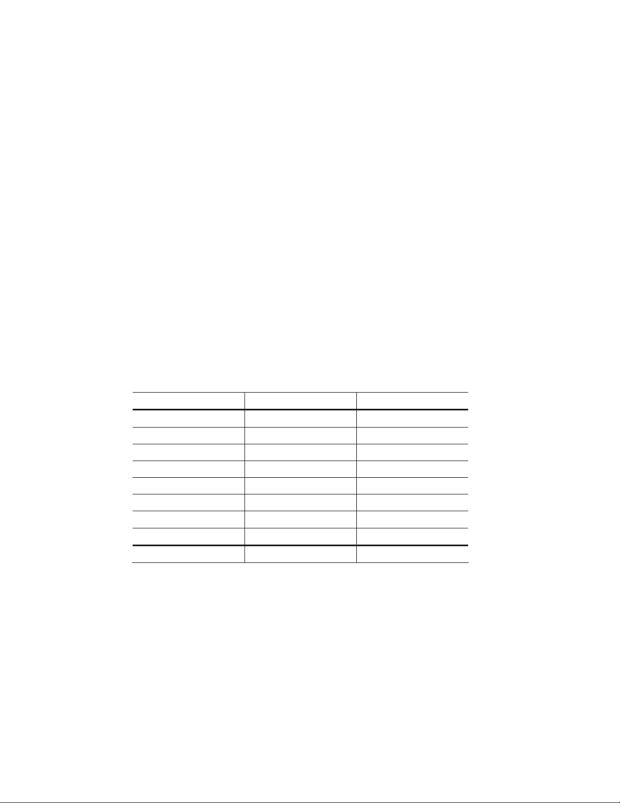
- [10pts] In a particular chip technology, an inverter driving Another, made of identical transistors has a propagation delay of 1ns for both 0Æ1 and 1Æ0 transistors.
The logic gates in the circuit below all are made of transistors identical to those in the inverters shown above. In the space below calculate the value of the critical path delay from either input (a,b) to the node labeled X. On the circuit diagram, label the delay associated with each gate on the critical path.
- [7pts] The NAND gates shown below are all made of identical transistors. Inputs signals as applied at node a and b and the resulting waveform at node c, are shown in the waveform diagram below. Neatly draw the waveforms for nodes d and e.
- a) [5pts] Shown below is a set of logic blocks used to implement carry look-ahead adders. In the space provided to the right of each one, write down the logic equation for every output of each block.
- [8pts] The circuit shown below is used to multiple the 6-bit number X by a 6-bit constant value C. It is made up of instances of a full-adder cell. The full-adder takes as input 3 1-bit signals and outputs a 1-bit sum and a 1-bit carry, as shown to the right.
What is the value of C?
- Shown below is an incrementer circuit. It accepts an N-bit input, X, and outputs X+1. It also has two enable signals, one input (ENin) and the other output (ENout), for controlling and extending the incrementer to larger sizes.
For large incrementers, this circuit suffers from excessive delay. One way to decrease the delay is to reorganize the circuit by applying the carry-select principle, used in fast-adder design for speeding up the carry signal.
a) [10pts] Sketch a block diagram of a 16-bit incrementer designed using the carry-select technique. Use 4 groups, all of the same number of bits. You may draw sub- incrementers as blocks, and may use simple logic gates and multiplexers as needed.
- [10pts] You are an engineer at AcmeVideo, Inc. Your current display system has the following specifications:
30 frames/second black & white display (only Y component for each pixel) 8 bits per Y component 600 pixels/line 600 lines/frame
The display system uses a frame buffer based on a SDRAM with the following specifications:
8-bit data interface 4+L cycles per read or write access, where L = burst length Maximum L = 6 48 MHz clock frequency
Your marketing department would like to bring out a new product based on your current display system. It will have a display monitor that can be rotated 90 degrees and a mechanical switch to detect when the monitor is rotated. When the monitor is rotated, the display system must rotate the video output by 90 degree to compensate. Your VP of engineering has decided that the cheapest way to achieve this compensation is to transform the image using the frame-buffer; it will be written to the frame buffer row-by-row, but read out column-by-column.
a) Using the existing frame buffer and changing the control logic, is it possible to support the rotation operation and maintain the display specifications? Show your work.
b) Adhering to all other specifications, what is the maximum frame rate when rotated?
- [10pts] Short answer.
a) [1pt] In Ethernet frames the CRC field is used for error detection, error correction, or both?
b) [1pt] Ethernet frames carry the “MAC” address of the sender, the receive, or both?
c) [1pt] True or false. Interlaced video display systems have twice the frame-rate as progressive scan systems.
d) [1pt] A 256 x 4-bit memory organized as a square array uses how many address bits for the row-decoder?
e) [1pt] A 256 x 4-bit memory organized as a square array uses how many address bits for the column-mux control?
f) [1pt] What size ROM is needed to implement a 4-bit adder with carry-in?
g) [1pt] How many 2-to-1 multiplexers are needed to implement a 4-bit universal shift register, based on d-type flipflops?
h) [1pt] The n-bit bit-serial multiplier takes how many cycles to produce the final result?
i) [1pt] The n-bit shift and add multiplier takes how many cycles to produce the final result?
j) [1pt] A Johnson counter with n states has how many flip-flops.