Download Output Expressions - Computer Engineering - Solved Exam and more Exams Computer Science in PDF only on Docsity!
4 problems, 5 pages Exam One Solution 9 February 2001
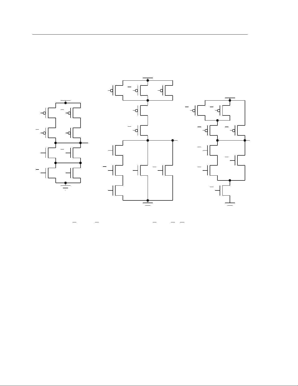
Problem 1 (3 parts, 30 points) Incomplete Circuits For each expression below, create a switch level implementation using N and P type switches. Assume both inputs and their complements are available. Your design should contain no shorts or floats. Use as few transistors as possible, but do not simplify the expression.
A
B B
A
A B
A B
Outx
A
D
B
A
Outy
C
E
B
C
D E
B
Outz
A
D
A
B
C
C
D
OUTx = A ⋅ B + A ⋅ B OUTy = (^) ( A + (^) B + C )⋅ D ⋅ E OUTz =^ (((^ A^ + B )⋅ C )+ D )
4 problems, 5 pages Exam One Solution 9 February 2001
Problem 2 (2 parts, 25 points) Mixed Logic In the year 3000, a Georgia Tech engineer opens a millennium time capsule that contains a gate design using mixed logic notation. “Great use of a common sub-expression!” she exclaims, “But you should have used NAND gates.” Extract the two output expressions from the circuit below and then reimplement using NAND gates. Determine the transistor savings of the new design. A B C D
E
OUTx
OUTy F
OUTx = (^) A ⋅( B ⋅ C + D )
OUTy = (^) ( B ⋅ C + D )+ E + F
NAND gate implementation (use correct mixed logic notation) A B C D
E
OUTx
OUTy F
Transistors in original implementation 5 x 4 + 6 x 2 = 32
Transistors in NAND implementation 5 x 4 + 2 x 2 = 24
4 problems, 5 pages Exam One Solution 9 February 2001
Part B (10 points) For the following behavior (in map format), derive a simplified sum of products expression using a Karnaugh Map. Circle and list the prime implicants, indicating which are essential. Then write the simplified SOP expression.
A
A
B B
C
C
C
D
D D
prime implicants
essential? yes no
A D
A B
A B
B D
A D
B D
simplified SOP expression (^) A ⋅ B + B ⋅ D + A ⋅ D or A ⋅ D + A ⋅ B + B ⋅ D
Part C (10 points) For the following behavior (in map format), derive a simplified product of sums expression using a Karnaugh Map. Circle and list the prime implicants, indicating which are essential. Then write the simplified POS expression.
A
A
B B
C
C
C
D
D D
prime implicants
essential? yes no A + D C + D A + C
simplified POS expression (^) ( A + D )⋅( A + C )