Download Logic Design -Components and Design Techniques for Digital System - Exams and more Exams Digital Systems Design in PDF only on Docsity!
EECS 150, Midterm 1, Fall 2005, Professor Randy Katz
Question 1. Combinational Logic Design (10 Points)
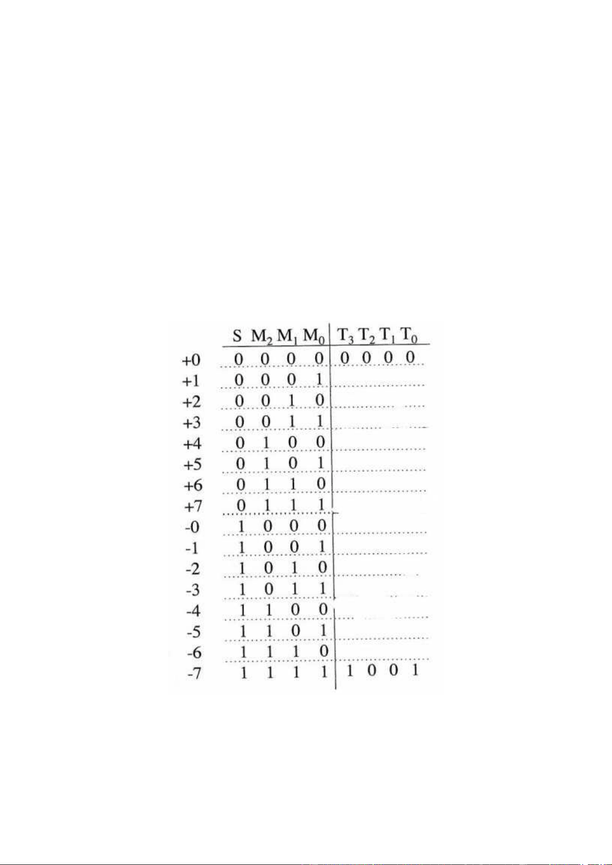
Your task is to design a combinational logic system to convert a four-bit “sign and magnitude number” (SM 2 M 1 M 0 ) to a twos complement number (T 3 T 2 T 1 T 0 ).
For example, 0111 2 , 1111 2 are the representations of +7 and -7 in sign and magnitude from respectively. In twos complement form, positive numbers are represented just like the sign and magnitude scheme, but the negative numbers are formed as follows. Take the positive form, complement the bits, and add 1. Thus, the representations for -7 in twos complement is formed as follows: 0111 2 -> 1000 2 -> +1 = 1001 2.
Note that sign and magnitude form has two representations for zero (1000 2 and 0000 2 ) while twos complement has only one zero (0000 2 ).
(a) To make sure that you understand the function to be implemented, complete the following truth table ( points).
(b) Fill in each of the four k-maps and minimize for sum of products implementation (8 points).
T 3 =
T 2 =
T 1 =
T 0 =
Question 3. Reverse Engineering (10 Points) Your task is to derive a PORTION of the state diagram associated with the following sequential logic circuit diagram:
(a) Is this a MEALY MACHINE or a MOORE MACHINE (circle one!) (1 point).
(b) Next, Write Boolean equations for the following circuit nodes (3 points): Z (A, B, QX, QY) = DX (A, B, QX, QY) = DY (A, B, QX, QY) =
(c) Next fill in the encoded state transition table (2 points):
(d) Based on your state transition table in part (c), complete the PORTION of the state diagram FOR THOSE TRANSITION ORIGINATING IN STATE 11 ONLY (i.e., there is no need to include transitions FROM states 00, 01, 10) (4 points):
Fill in the following behavioral Verilog fragments: (a) The high order bit slice D[3] (4 points):
always @(posedge clk)
case (OP)
3’b000: D[3] <=
3’b001: D[3] <=
3’b010: D[3] <=
3’b011: D[3] <=
3’b100: D[3] <=
3’b101: D[3] <=
3’b110: D[3] <=
3’b111: D[3] <=
(b) The low order bit slice D[0] (3 points):
always @(posedge clk)
case (OP)
3’b000: D[0] <=
3’b001: D[0] <=
3’b010: D[0] <=
3’b011: D[0] <=
3’b100: D[0] <=
3’b101: D[0] <=
3’b110: D[0] <=
3’b111: D[0] <=
(c) A middle bit slice D[i]. Write you answer in terms of D[i], D[i+1], and D[i-1]. (3 points)
always @(posedge clk)
case (OP)
3’b000: D[i] <=
3’b001: D[i] <=
3’b010: D[i] <=
3’b011: D[i] <=
3’b100: D[i] <=
3’b101: D[i] <=
3’b110: D[i] <=
3’b111: D[i] <=
Question 5. Latch vs. Edge-Triggered Storage Element Behavior (10 points)
Device A is a clock-level sensitive R-S latch (i.e., it reacts to the R-S inputs only when the clock is high). Device B is an R-S Flip-Flop that is positive edge triggered. Device C is an R-S flip-flop that is negative edge triggered.
Assume 0 set-up and hold times, and 0 propagation delays. All devices treat R and S as active high signals (i.e., Reset when R is true and Set when S is true), and are implemented using NOR gates. Initially the devices have 0 stored in them.
Complete the timing diagram below for the signals QA, QB, QC, showing the behavior of the three different device to the same R and S input changes: